Engineering brilliance:
HPA sapphire a platform
for LED production
High purity alumina sapphire has many benefits that make it a vital component in LED production
Giant LED displays light up New York’s Times Square. © Pexels, Marcus Herzberg
HIGH purity alumina (HPA) is a material you may
not have heard of, but it is an important ubiquitous
component of our daily lives. It is the primary
ingredient in the production of sapphire crystals,
which are fundamental to light-emitting diodes
(LEDs) – small light sources that illuminate everything
from our personal devices to our cities.
The demand for HPA is on a steady rise owing to the
increase in demand for sapphires, driven by the LED
industry. The value of sapphires as a material for LED
production can be condensed into the following four
key reasons:
Firstly, sapphire shares a similar crystal lattice
dimension with gallium nitride (GaN), the primary
material used in the creation of high-brightness blue
and white LEDs. This lattice compatibility results
in fewer structural defects, thereby enhancing the
efficiency of the LED production.(1)
Similarly, transparency is another crucial feature,
ensuring the light generated faces no obstruction
from the LED’s underside, giving sapphire an
advantage over silicon as an LED substrate.
Moreover, sapphire’s high thermal conductivity is
vital for LEDs, which generate heat during operation.
Efficient heat dissipation is necessary to prevent damage to the LED structure and maintain its
lifespan and efficiency.
Lastly, sapphire’s superior electrical insulation
properties allow it to effectively insulate the active
parts of the LED from other components, reducing
the risk of electrical short circuits.
The journey from high purity alumina to an LED
is complex and fascinating, involving a blend of
chemistry, engineering and precision manufacturing
that often spans across international borders.
The genesis: High purity alumina
The production chain commences with HPA – a
superior-grade aluminium oxide (Al2O3) powder,
produced with a focus on purity. 4N HPA (99.99%
pure) is typically employed for LED applications,
while an even purer variant, 5N HPA (99.999% pure),
is used for optics.
The purity of HPA is not merely a number, it’s the
cornerstone of successful LED production. Even
the slightest impurity can induce defects in the final
product, impacting the performance and efficiency of
the LEDs.
LED production, for example, is very sensitive to
the effects of Low Angle Grain Boundaries (LAGBs) – small crystal grains in the sapphire wafer that are
misaligned compared to the main wafer volume.
They reduce adhesion and compromise the structural
quality of the epitaxial layer deposited on the
sapphire wafer, reducing LED device performance.
The purity of the HPA has a direct influence on the
occurrence of such defects.
Another factor that is becoming increasingly
important for HPA users is maintaining a green
supply chain with no carbon emissions.
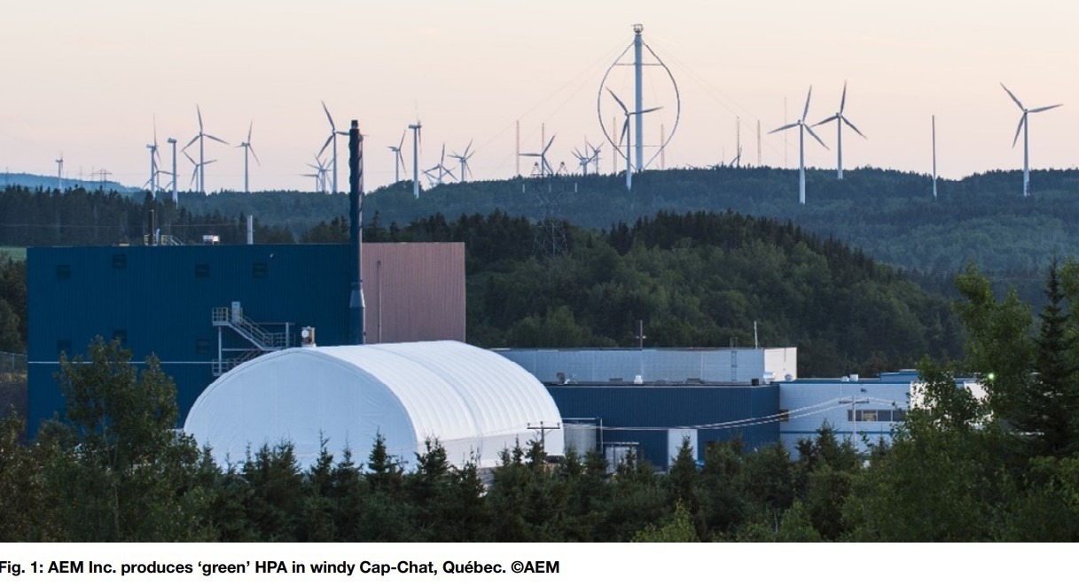
In the quest for a high-purity and environmentally
friendly high purity alumina, companies like
Advanced Energy Minerals, based in Cap-Chat,
Québec, Canada, (Fig. 1 ) are leading the way. The
company sources raw material exclusively from
hydropower and is committed to 100% green HPA
production, powered exclusively by green energy
from Q3 2023.
The birth of sapphire crystal: A process of precision and patience
The production of synthetic sapphire crystals, known
as ‘boules’, from HPA powder or monoliths is a
complex process where size matters.
Sapphire boules serve as the starting material for
thin wafers (250-150 µm) that later become LED
substrates during production. The diameter of the
finished LED wafers is determined by the size of
the boules. This diameter can range from 2” (almost
obsolete now) to 6-8” (common today) to 12” (future
standard).
Competition requires growing larger boules, which is
more economically viable.
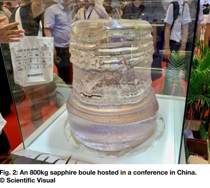
For context, a 90kg boule that accommodates an
8” core diameter, has a bottom diameter of 30cm
and stands at 45cm tall. The largest sapphire boule
produced at the time of writing is 800kg and measures
70-80cm tall. It was manufactured in China (Fig. 2).
Growing such boules demands precision, expertise, and time. The LED sapphire is often produced using the Kyropoulos growth method,(2) which allows the largest crystals of the highest quality to be produced.
The process begins with a slightly imperfect sapphire seed coming into contact with high purity alumina melt at around 2,050°C (3,686°F). As the crystal grows, it is surrounded by the melt and continues to grow until its surface reaches the crucible walls and gets lifted to restart the growth cycle. This method allows crystallisation at low temperature gradients, resulting in lower thermal stresses in the crystal.
Sapphire growth requires an experienced operator
who is trained for several months. For a 90kg boule,
the process takes 17 days – 8.5 days to grow the
crystal and another 8.5 days to cool it down, and for
800kg it is far more than a month.
Sustainability is also a key component of this
process, as the crystal-growing furnace can
consume 200 kW of electricity or even more.
Sapphire manufacturer Alox Technology, based in
Washougal, Washington State, uses hydroelectric
power from the nearby Columbia River for the
crystal growth. This is an example of how the LED
industry not only produces products with low power
consumption but also promotes environmental
sustainability.
Diving deeper: The art of coring and wafering
The growth of a boule is merely the beginning of the
journey. For the boules from Alox Technology, this
journey leads from the West Coast of the US to Riga,
Latvia.
In order for the boule to become a LED substrate,
it must first be processed into a cylindrical core, or
‘cored’.
But before that, it must be ensured that the parts of
the boule volume that are used for wafer production
are free of defects such as small bubbles, cracks,
and impurities. This is where the company Scientific
Visual from Switzerland come in, offering advanced
crystal inspection equipment.
Scientific Visual’s fully automated four-axis scanners inspect large sapphire boules and detect internal
defects with an accuracy down to 8 µm. These
scanners can identify bubbles, structures, clouds,
and other yield-impacting defects and encode them
in a 3D model called a digital twin. This digital twin
enables computer-aided optimisation to determine
the defect-free zones that are most suitable for
processing (Fig. 3 ). This maximises yield in both the
coring and wafering processes.
For example, if there are few defects in an extracted
core, their positioning relative to the wafering
system is important. If you know the exact defect
co-ordinates, you can calculate a core offset in
the wafering machine to position more defects in
the saw gaps and outside the future wafers. Such a
defect-aware wafering approach, known as Smart
Wafering, enables up to a double-digit increase in
defect-free wafer production without the need to
grow or buy new boules.(3) The only prerequisite for
this is a high-precision digital twin of the crystal.
After coring, the extracted cylinders are ‘wafered’
into thin slices that are about 300-800 microns
thick, depending on the diameter. Sapphire has a
hardness just below that of diamond, so diamond
saws and considerable energy is used for cutting and
wafering. The wafers are then further refined through
processes such as grinding and polishing to prepare
them for the next phase of their life in an LED.
The finishing touches: From wafer to LED
After the rigorous process of inspecting and cutting,
the sapphire boule is transformed into thin wafers
that serve as the LED epitaxy. Each wafer is placed in a chamber heated to 900°C to grow the light-emitting
layers on it, taking advantage of the sapphire’s hightemperature stability.
The LED layers are usually made of GaN, AlGaN
and InGaN. These materials have thermal expansion
coefficients and chemical resistances that must
be very similar to those of the sapphire wafer. The
interfacing of sapphire and light-emitting layers is the
result of years of research and development.
After growing the LED layers, the wafer goes through
a series of steps such as lithography, masking and
etching to bring the individual units, the so-called
‘dies’, to the desired size, followed by the application
of electrical contacts. The LEDs are then sawn and
packaged and mounted directly on an electronic
circuit board.
Throughout the whole process, precision is key.
Every step, from the creation of the high purity
alumina to the final LED production, has an impact
on the quality of the final product. As we move
towards the production of smaller devices such as
micro-LEDs, these steps need to become even more
precise to match the miniaturised dimensions.
With that miniaturisation, the industry is facing
stricter standards for the final products. This
ripple effect on the end products gets to the first
production steps, such as high purity alumina
production.
The future of HPA and LED production: Lighting the path forward
The world of LEDs is not static; it’s continually
evolving and improving. The evolution goes to
smaller devices with higher brightness.
A close relative of the LED, the miniLED, is
characterised by its smaller size. A miniLED
measures between 100 to 200 micrometres on a
side,(4)
which, while smaller than a typical LED, still
packs a powerful punch in terms of brightness and
efficiency.
The future of display technology is often associated
with microLEDs. Although they currently find a
home primarily in high-end displays due to their high
production costs, their potential is immense.
Each subpixel (or diode) in a microLED display is
individually controlled, emitting light without a backlight,
similar to an OLED display.(5)
Sizes of microLEDs
can range down to 3 µm, with a typical microLED
measuring around 10 µm. To put that into perspective,
a human hair is typically 70 +/- 20 µm thick.(6)
The LED industry is a dynamic and rapidly evolving field, with new technologies and applications
emerging regularly. As the demand for more efficient,
brighter, and smaller light sources continues to grow,
the role of HPA and sapphire in the LED industry will
only become more critical.
In 2022, the projected total volume of high purity
alumina was approximately 35,000 tons, with
a substantial 30,000 tons designated for LED
production.
Looking ahead to 2025, the demand for HPA
is expected to rise to 58,000 tons, with LEDs
accounting for a significant 49,000 tons, or an
impressive 84% of the total. By 2028, the demand
for LEDs is forecasted to reach a remarkable 85,000
tons.(7)
In essence, LEDs have been and will continue to be,
a crucial market for HPA, even as new applications
emerge and other markets expand.
As for sapphire, the global market for these crystals
attained a value of $903.3m in 2021, according to the
IMARC Group. They anticipate this figure to escalate
to $2,471.4m by 2027, with a CAGR of 18.5% during
the period from 2022 to 2027.(8)
Authors
• Richard Foster, Advanced Energy Minerals Inc.
• Mark Fearns, Advanced Energy Minerals Inc.
• Lauris Dimitrocenko, Alox Technology
• Ivan Orlov, Scientific Visual
• Caroline Chèze, Scientific Visual
• Mark Fearns, Advanced Energy Minerals Inc.
• Lauris Dimitrocenko, Alox Technology
• Ivan Orlov, Scientific Visual
• Caroline Chèze, Scientific Visual
References
1. Chao, Yeh, Wu, Kawagashi, Hsu, RSC Adv., 2020,10, 16284-16290 at
https://pubs.rsc.org/en/content/articlelanding/2020/ra/d0ra01900c
2. https://www.substech.com/dokuwiki/doku.php?id=synthetic_
sapphire#kyropoulos_method
3. https://www.youtube.com/watch?v=WFowrwiCnvo
4. https://encyclopedia.pub/entry/11217
5. https://www.radiantvisionsystems.com/blog/microled-cusp
6. https://wowskinscience.com/blogs/news/how-thick-is-human-hair
7. microled.info.com – 2022; Emergen Research – LED report 2022; CRU
Research – HPA Report 2021
8. https://www.imarcgroup.com/sapphire-glass-market, 2021