HPA transforms into the vital sapphire components integral to LED and
watch cover production by enhancing its quality and sustainability.
Environmental costs are in the focus of sapphire production, which can
be minimised by using low-emission HPA produced by Advanced Energy
Minerals/CA.
Sapphire – a material with outstanding properties.
Sapphire is a key component to our everyday life due to its transparency, scratch resistance, and high thermal conductivity.
These properties make it ideal for various uses, such as scratchproof windows,
translucent ceramics and insulating layers
for semiconductors. A sizeable quantity of sapphire is used to make jewellery and watches, where recent trends have lead to a higher demand from consumers for sustainable products.
Manufacturing HPA starts with a mineral
feedstock. If this feedstock is manufactured
with hydropower as the only energy source,
its only carbon impact occurs from the
transportation. If the mineral source is close
to the factory, this can be minimal or even
brought to zero by compensation
Such is the case for Advanced Energy Minerals (AEM) which manufactures HPA in
Québec/CA; a region blessed by ubiquitous
hydroelectric infrastructure utilising regional feedstock produced predominantly with
hydroelectric power.
The report is in accordance with the classification proposed by the Greenhouse Gas
Protocol (GHG Protocol).
This is in strong contrast to alumina producers using the traditional alkoxide processes,
who typically have very poor utilisation of
renewables, which emits 12,3 t of CO2
per
ton of HPA. Other producers have a goal
of reducing this by a factor of five, which
is still very high. AEM has also a product
line to deliver customised 4N (99,99 %)
and 5N (99,999 %) purity compacted alumina monolithics to its customers. These
ranges in size from pucks of a few grams to
giant pucks of up to 21 kg. 4N HPA is typically employed for LED applications, while
an even purer variant, 5N HPA, is used for
optics.
The processes to convert HPA to sapphire
all melt the alumina at a temperature above
2050 °C. This is followed by a slow cooling process that takes one to two weeks to
create a crystal of sapphire. Because this is
a relatively low-tech process, the crystal is
not perfect. It can, however, be influenced
by the quality of the HPA used and the dexterity of the furnace operator. Lower-purity
HPA is used for LEDs.
The next level of purity finds application
in watch covers. The highest quality HPA
is transparent to deep UV due to its low titanium content. This makes it suitable for
medical applications.
Crystallisation issues may also impact the
final product quality and determine the final application. For instance, an LED device
containing an imperfect and inhomogeneous sapphire component may experience
decreased efficiency, a shorter lifespan, or
a variation in emitted colour. In addition to
HPA quality, the different sapphire growing
processes yield crystals that are suitable
for different applications.
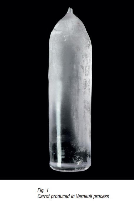
Sapphire “carrots” for watch covers
Sapphire crystals for watch covers are
traditionally grown with the Verneuil process. The result that awaits further processing is called a “carrot” in the trade
(Fig. 1). It is close to a cylinder in form,
approximately 15 cm high and 3–4 cm in
diameter. Of course, this step has a typical energy requirement if not performed
with green energy. The relevant CO2
emission would be an average of 89 g/kWh for
Switzerland, where environmental issues
have a strong focus, or 475 g/kWh worldwide.
Because the crystal sapphire carrot has an
imperfect form and contains defects, there
will be substantial yield loss during the
further processing steps. This loss can be
minimised by generating a digital model of
the carrot that is based on a 3D scan with
specialised confocal tomography equipment.
It is worth noting that cutting and polishing
sapphire is highly energy-consuming, as
the material’s exceptional hardness presents a significant challenge. The first step
with yield loss is the scrapping of carrots after inspection and before further processing due to an unacceptable rate of defects.
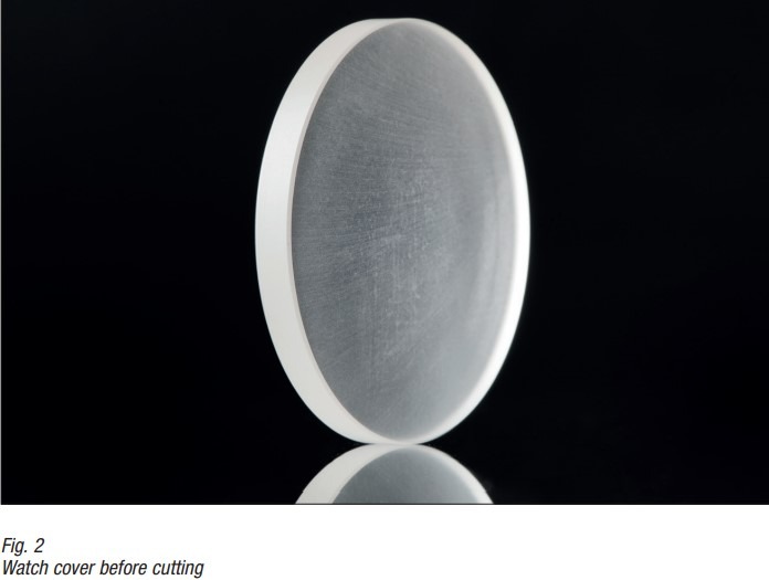
The yield from slicing the core into wafers
and polishing them is 85 %. The result is
an average combined yield of 28 % in
the watch industry for a flat watch cover
(Fig. 2). This will have a diameter ranging
from 25–45 mm and a thickness from 1,6–
6 mm. The typical weight is 4,6 g.
These steps can all be optimised with
digital quality control from the Swiss company Scientific Visual. The company manufactures scanners for quality inspection of
industrial crystals. Using these automated
tools, individual steps can be optimised
to avoid defects. For example, it prevents
defective crystal parts from entering costly
processing. In addition, by providing feedback to crystal growers, fewer crystals will
have to be scrapped. The simulated form
for the cylinder can be moved so that a
minimum of defects remain in the physical
carrot. Slicing can also be offset to bring
defects between adjacent wafers. These
steps all work to bring the yield for a flat
cover to 34 %. For a domed watch cover,
the improvement is from 4 % to 5 %, which
is a 25 % improvement
Effect of low-emission HPA from AEM for
watch cover production is considerable. In
the worst-case scenario, HPA emits 12,3 g
of CO2
per g of HPA. Manufacturing the flat
watch cover emits: 12,3 g× 4,6 g/0,28
yield = 202 g and the domed watch cover
emits: 12,3 g × 4,6 g/0,04 yield = 1400 g.
The use of current low-emission HPA and digital quality control reduces these values
to 20 g and 138 g, respectively. This is even
before zero-emission HPA eliminates the
cost completely, if not the wastage.
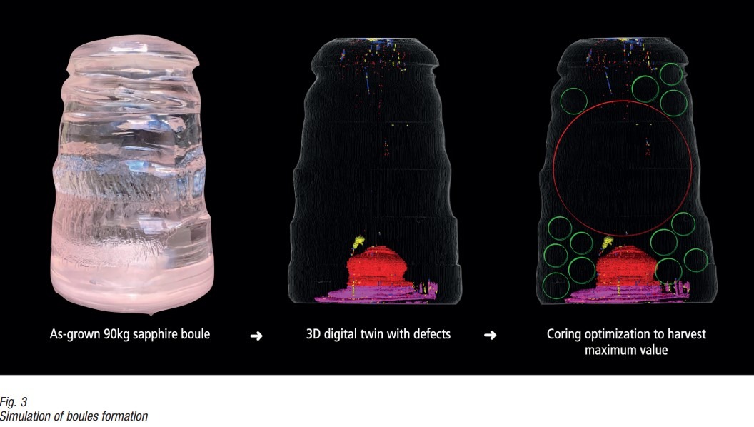
Sapphire “boules” for LEDs
The production of synthetic sapphire crystals, known as “boules”, from HPA powder
or monoliths is a complex process where
size matters (Fig. 3). Sapphire boules serve
as the starting material for thin wafers
(250–150 μm) that later become LED substrates during production.
The diameter of the finished LED wafers is
determined by the size of the boules. This diameter can range from 2″ (almost obsolete
now) to 6–8″ (common today) to 12″ (future
standard). Competition requires growing
larger boules, which is more economically
viable. For context, a 90 kg boule that accommodates an 8″ core diameter, has a bottom diameter of 30 cm and stands at 45 cm
tall. The largest sapphire boule produced at
the time of writing is 800 kg and measures
70–80 cm tall. It was manufactured in
China.
Growing such boules demands precision,
expertise, and time. The LED sapphire is often produced using the Kyropoulos growth
method, which allows the largest crystals of
the highest quality to be produced. The process begins with a slightly imperfect sapphire seed coming into contact with high purity alumina melt at around 2050 °C. As
the crystal grows, it is surrounded by the
melt and continues to grow until its surface
reaches the crucible walls and gets lifted to
restart the growth cycle.
This method allows crystallisation at low
temperature gradients, resulting in lower
thermal stresses in the crystal. For a 90 kg
boule, the process takes 17 days – 8,5 days
to grow the crystal and another 8,5 days to
cool it down, and for 800 kg it is far more
than a month.
Sustainability is also a key component of
this process, as the crystal-growing furnace can consume 200 kW of electricity
or even more. Sapphire manufacturer Alox
Technology, based in Washouga/US, uses
hydroelectric power from the nearby Columbia River for crystal growth.
This highlights how the LED industry not
only produces products with low power
consumption but also promotes environmental sustainability.
In order for the boule to become a LED
substrate, it must first be processed into a
core, or “cored”. But before that, it must be
ensured that the parts of the boule volume
that are used for wafer production are free
of defects such as small bubbles, cracks,
and impurities. This is where the company
Scientific Visual from Switzerland come in,
offering advanced crystal inspection equipment.
After coring, the extracted cylinders are
“wafered” into thin slices that are about
300–800 µm thick, depending on the diameter. Sapphire has a hardness just below
that of diamond, so diamond saws and
considerable energy is used for cutting
and wafering. The wafers are then further
refined through processes such as grinding
and polishing to prepare them for the next
phase of their life in an LED.
After the rigorous process of inspecting and
cutting, the sapphire boule is transformed
into thin wafers that serve as the LED epitaxy. Each wafer is placed in a chamber
heated to 900 °C to grow the light-emitting
layers on it, taking advantage of the sapphire’s high-temperature stability.
With that miniaturisation, the industry is
facing stricter standards for the final products. This ripple effect on the end products
gets to the first production steps, such as
high purity alumina production. A close
relative of the LED, the miniLED, is characterised by its smaller size. A miniLED
measures between 100–200 µm on a side,
which, while smaller than a typical LED, still
packs a powerful punch in terms of brightness and efficiency.
The future of display technology is often
associated with microLEDs. Although they
currently find a home primarily in high-end
displays due to their high production costs,
their potential is immense.
The future of display technology is often
associated with microLEDs. Although they
currently find a home primarily in high-end
displays due to their high production costs,
their potential is immense.
Market forecast for sapphire and HPA –
Green Alliance for Sapphire
The LED industry is a dynamic and rapidly evolving field,
with new technologies and applications emerging regularly.
As the demand for more efficient, brighter, and smaller light
sources continues to grow, the role of HPA and sapphire in
the LED industry will only become more critical.
In 2022, the projected total volume of high purity alumina
was approx 35 000 t, with a substantial 30 000 t designated
for LED production. Looking ahead to 2025, the demand for
HPA is expected to rise to 58 000 t, with LEDs accounting for
a significant 49 000 t, or an impressive 84 % of the total. By
2028, the demand for LEDs is forecasted to reach a remarkable 85 000 t.
In essence, LEDs have been and will continue to be, a crucial
market for HPA, even as new applications emerge and other
markets expand.
As for sapphire, the global market for these crystals attained a value of USD 903,3 million in 2021, according to
the IMARC Group. They anticipate this figure to escalate to
USD 2471,4 million by 2027, with a CAGR of 18,5 % during
the period from 2022 to 2027.
With this growth potential it is relevant to watch the carbon
foot print of the processes involved.
A project called Green Alliance for Sapphire, is a kind of consortium of companies active along the sapphire glass value
chain that acknowledge that sapphire is not a sustainable
product and its production causes significative carbon emissions. Moreover, the partners in the alliance are committed
to working to bring to the market a more sustainable sapphire, and by doing so, contributing to the decarbonization
of the industry. For AEM it is important to be in this network.
[1] OPTEL Carbon footprint assessment report for Advanced Energy (upon request)